What’s the Next Big Thing at Samsung Displays?

Image Credit: Courtesy Samsung Advanced Institute of Technology
It’s the kind of breakthrough any lab hopes for — one that starts with a current technology and discovers a revolutionary way to take it to an unexpected level.
Researchers at Stanford University and the Samsung Advanced Institute of Technology (SAIT) developed a proof of concept for a metaphotonic display technology that could improve the color purity of existing OLED screens — by potentially boosting the pixel density to a whopping 10,000 pixels per inch (ppi).
Today, when we talk about displays, we say Full HD is 1920×1080 pixels or 4K is 3840×2160 pixels. But counting the total number of pixels for resolution only tells one story of picture quality.
Pixel count focuses on the number of pixels across the length and width of a digital image — that is, the image dimensions in pixels. It’s about size.
PPI, or pixels per inch, refers both to the counts the fixed number of pixels that a screen can display and the density of pixels within a digital image.
Pixel-dense metaphotonic display is already more than a theory. You can hold the lab’s proof in your hands in the footprint of a small device. Yet this is Next-Big-Thing (NBT) technology as the tech will still need to be scaled for use in a full-size display.
To develop this new architecture for OLED, Stanford researchers and Samsung collaborators in Korea borrowed and repurposed existing designs for electrodes of ultra-thin solar panels. (The thought being, “Well if it works for solar panels, maybe it could be done with OLED.” You could say, researchers “saw the light.”)
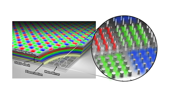
The team added an extra layer to the bottom of a conventional OLED stack, an optical metasurface bespeckled with nanoscale (smaller than microscopic) corrugations. These manipulate the way the light reflects back, changing how the different colors resonate in each pixel.
“We’ve taken advantage of the fact that, on the nanoscale, light can flow around objects like water,” said lead researcher Mark Brongersma.
Their metasurface manipulates the reflective properties of light, allowing different colors to resonate in the pixels and facilitating effective light extraction from the OLEDs. The lab compares this to the way musical instruments use acoustic resonances to produce more beautiful (and easily audible) tones.
Researchers think this should facilitate a simpler manufacturing process for large-scale as well as micro-scale fabrication.
When compared to OLED tech found in today’s large displays, the new “metaphotonic device” retains a higher color “purity” and had twice the luminescence efficiency (the ratio of its brightness to energy efficiency). And of course, there’s also the benefit of the 10,000-ppi pixel density. With that many pixels crammed into a display, it’ll show stunning images with a level of detail close to the real world.
Thanks to the innovation in solar panels, this will also be vital research for VR/AR/MR headsets, where it has been easier to spot the gaps between the pixels. If they’re too wide, you’re looking into the virtual world through a screen door.
It will be a few years, but Samsung might soon be able to add The Meta-OLED to The Wall, The Frame, The Sero …


